DDR Tool#
This section introduces the DDR configuration and validation tool, which is an embedded componen of Config tools for i.MX.
The DDR tool provides two main functionalities: configuration and validation.
Supported devices are indicated in the new project configuration page.
Note: DDR tool is provided “as is” to aid customer capabilities of evaluating, debugging, and optimizing their designs. The results, or any part thereof, provided by the tool cannot be under any circumstances seen as a substitute for the traditional validation and compliance methods, which still need to be performed to declare compliance of the designs with the respective JEDEC standards.
Create a new DDR tool project#
To use the DDR tool, you first must create a new project.
To create a new DDR tool project, follow these steps:
Open the Config tools for i.MX.
Choose Create a new standalone configuration for processor, board, or kit and click Next.
From Processors, choose one of the devices with DDR tool support and click Finish.
To open the DDR tool view, click the DDR tool icon.
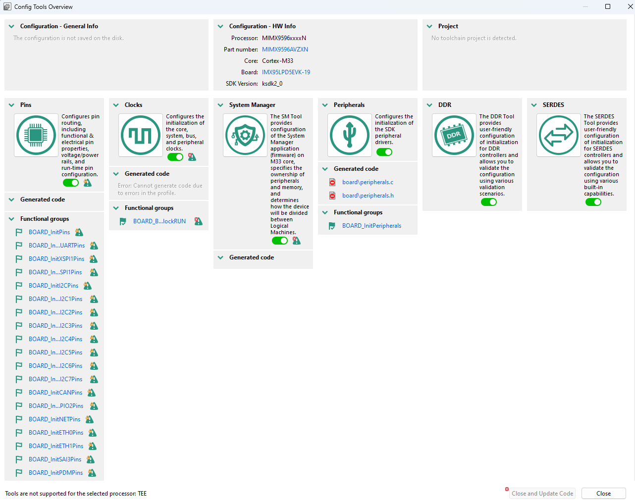
Config Tools overview#
To use the DDR tool, accept the Disclaimer.
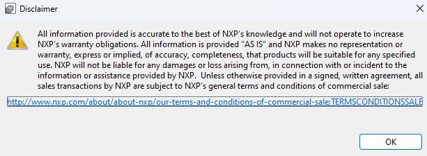
Disclaimer#
DDR configuration#
The DDR configuration provides a user-friendly graphical interface to configure the DDR interface and other associated subsystems. You can use it to change the DDR controller and PHY configuration when a different memory module is used to the configuration and to optimize the parameters associated with signal integrity.
Import initialization script#
Import initialization script allows loading the initialization script provided by the Register Programming Aid (RPA) tool and bypassing the UI configuration. To obtain the latest RPAs, refer to the following link on NXP community.
To import the RPA initialization script, use the Import initialization script button and browse for the desired *.ds file
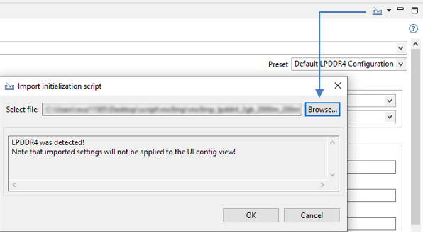
Import initialization script#
To load the *.ds file and disable the UI configuration interface, press OK.
Disabled UI#
The contents of the imported *.ds file is shown in Code Preview, ddr_config.ds
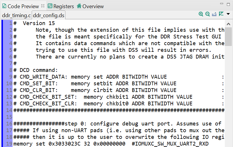
RPA script content#
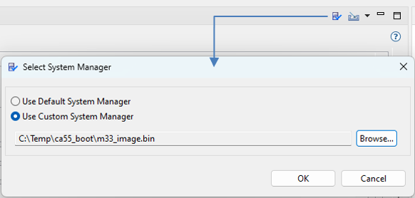
Select custom System manager#
In case of processors with the System manager, the default EVK board is supported by the DDR tool. For custom boards, the System manager for that specific board must be selected to be able to run memory tests.
To select a custom System manager, use the Select System Manager button, select Use Custom System Manager and browse for the custom System manager binary.
Note: Modify the SM configuration configs/customer_board.cfg
In the A55 non-secure section:
Make the LM owner of the
DDR_CTRL, DDR_PHY, SRC, andSYSCTR_CTLresources# Resources … DDR_CTRL OWNER DDR_PHY OWNER SRC OWNER SYSCTR_CTL OWNER
Grant the full DDR access to the LM:
# Memory EXEC, begin=0x080000000, end=<highest DDR address>
Make sure that the UART1 is dedicated to the A55 LM, as the A55 test code uses this UART. This is the default in the NXP EVK SM configuration (SM uses UART2), but customers may have changed this.
Select System manager#
To revert to EVK default System manager, select the Use Default System Manager option.
Enable manual configuration#
To switch back to UI configuration, press the button “Enable manual config”.
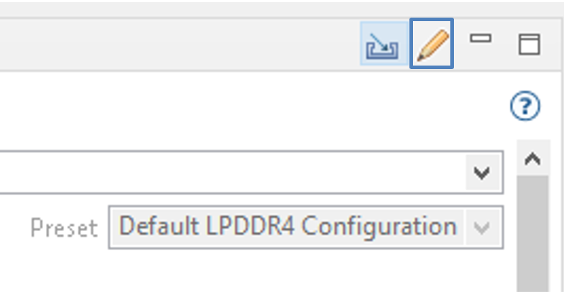
Enable manual config#
UI configuration#
The UI configuration allows you to change manually Device Information, PHY options, or Design-specific configuration. There are two modes available, Basic and Advanced.
Note: Advanced mode is only recommended for experienced users.
Basic mode allows you to configure the parameters that are design-dependent.
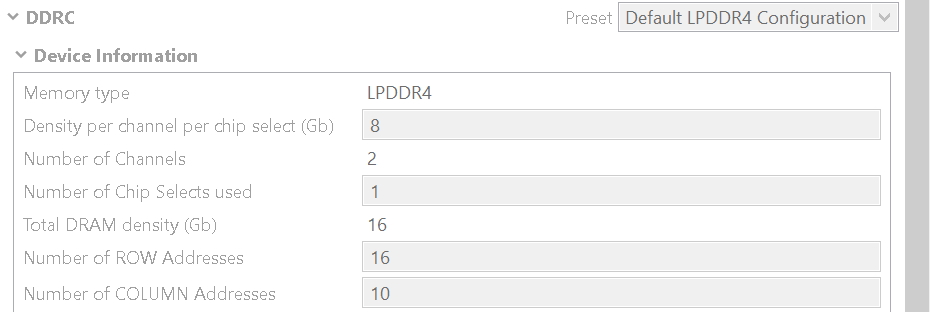
Device information
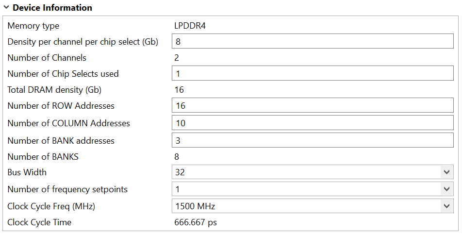
Device Information UI#
Board data bus configuration for LPDDR4
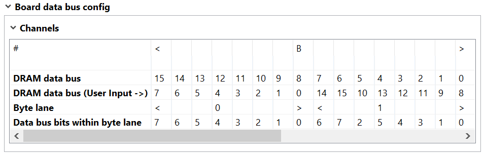
Board data bus config UI#
UART port selection

UART selection UI#
DBI selection (for LPDDR4)

DBI selection#
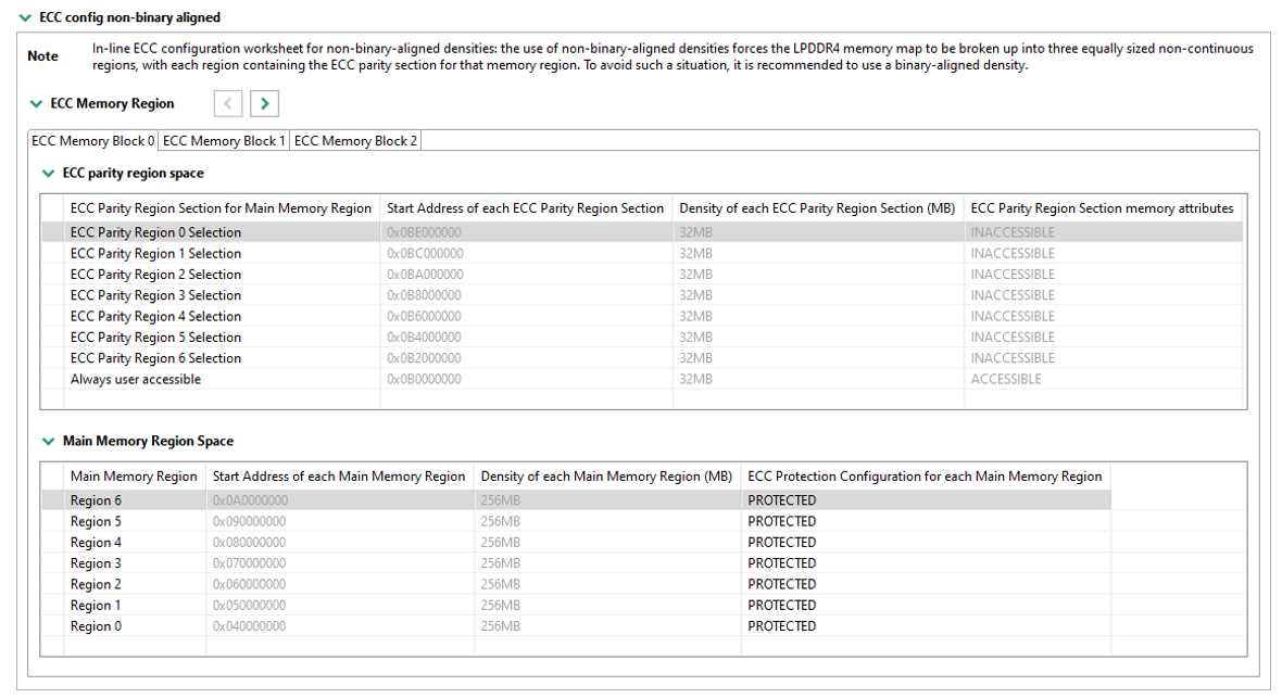
Inline ECC configuration (for devices with Inline ECC support) allows selection of the following parameters:


Advanced mode allows you to configure additional parameters.
The firmware version is the one officially supported by the BSP, but the DDR tool offers the possibility to select between multiple versions.

Firmware version selection UI#
Note: Use only the Firmware version for your specific SoC and BSP GA version. Not all Firmware versions are supported for each SOC.
PHY log level selection

PHY log level selection#
IOMUX configuration

IOMUX configuration UI#
PMIC configuration sequence
Note: In case the Custom PMIC initialization option is enabled, the available commands are:
pmic_set: most significant byte is the register, followed by the valuepmic_cfg: most significant byte is the I2C bus, followed by the I2C address.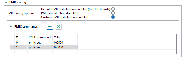
PMIC configuration UI#
Custom configuration
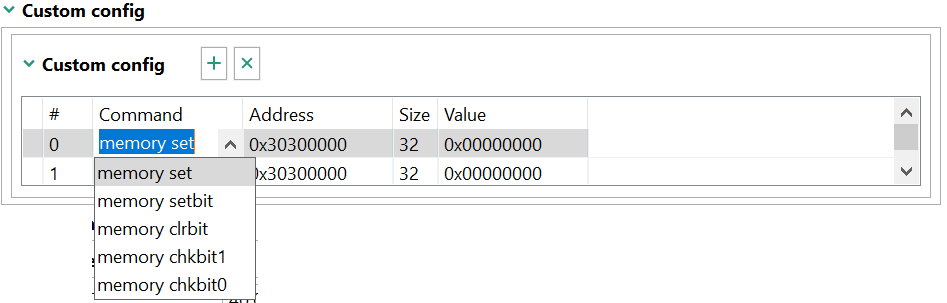
Custom configuration UI#
Note: Any write to an incorrect address may cause unexpected behavior.
DQ ODT and DS configuration

DQ ODT and DS configuration UI#
CA ODT and DS configuration – Informational Only

CA ODT and DS configuration UI#
Code generation#
You can generate the configuration as C code in the Code Preview View, which can be used by the U-Boot SPL driver.
You can trigger code generation by any change in the GUI, it is highlighted in the Code Preview.
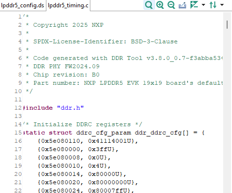
Code Preview#
You can save files from Code Preview on the disk by using DDR tool Export Wizard.
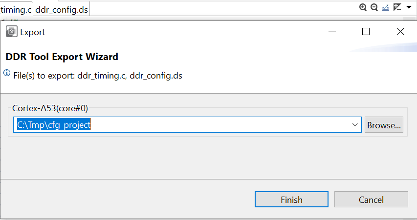
Export generated files#
DDR validation#
The DDR validation uses different scenarios to assess DDR performance, by downloading a test image to the processor’s internal RAM.
DDR validation can help to assess stability of the DDR interface on the board in a non-OS environment.
DDR validation#
Connection#
This section describes connection to boards of various types.
Boards with Serial Download mode/Manufacture mode#
To connect to a board, do the following:
Configure the board to boot in the Serial Download mode/Manufacture mode and power up the board.
Connect a UART cable from the host computer to the UART of the A-core on the board.
Connect a USB cable from the host computer to the USB port on the board that is used by the Serial Download mode. An “HID-compliant device” or a “USB Input Device” is shown in the Windows Device Manager.
Note: It is highly recommended to connect the USB cable directly to the Host PC USB port and not through a USB HUB.
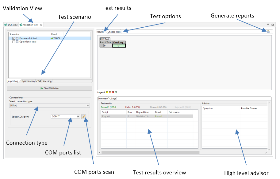
With the board connected to the host computer, search the UART ports by using COM port scan. COM port drop list is populated with all the available UART ports.
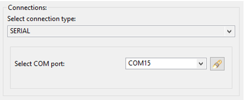
COM port selection#
Choose the correct UART that is used as the A-core debug UART port.
Boards with JTAG connection available#
Connect the JTAG probe (only the CWTAP probe is supported) to the board.
Select between USB or Ethernet connection.
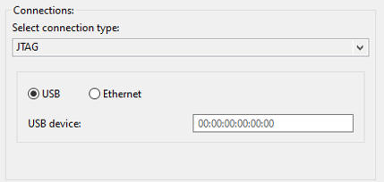
Connection type selection#
Test scenarios#
Once the DDR configuration and board connection are set up, you can execute different Test scenarios. You can customize each test by setting the parameters from Test options.
Depending on the test and options selected, the execution time may differ. By default a 90 seconds timeout is set, to assure that in case of an issue the test finishes. To change the default value, edit the Timeout (seconds) option:
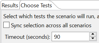
Timeout selection#
When initial timeout expires, provide the input to continue or not the test execution.
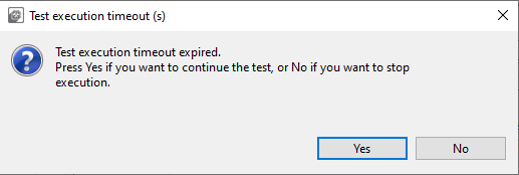
Test execution timeout(s)#
To start test execution, press the “Start Validation” button. You can check the status of the running test from the Logsconsole. By default, the log level is set to ERROR. Additional log-level options are available, with different output in the console:
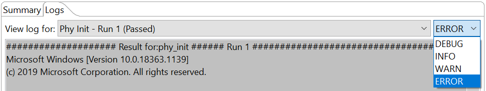
Log level selection#
At the end of the test, the PASS/FAIL status is displayed in “Results”. The test summary is displayed in “Summary”.
Test status#
Yellow is for Test failed
Orange is for Configuration error
Red is for Target connection error or exception in the script
Green is for Test passed
If a test fails, the Summary view in the Advisor section displays Symptom and Possible Causes to provide high-level guidance on the debug process when looking for possible DDR subsystem issues.
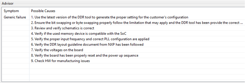
Advisor section#
The DDR tool offers several test scenarios that can be split into Inspection, Optimization, vTSA, and Stressing.
Inspection#
Inspection shows the status of the DDR Controller and DDR PHY configuration, by executing following tests:
Firmware Init – executes the DDR PHY training to check the DDR PHY configuration.
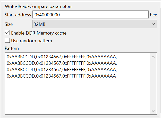
Operational – performs basic memory access test by running Write-Read-Compare/ Walking Ones/ Walking Zeros tests. Such options as Start Address, Size, Enable DDR Memory cache, Access mode/Pattern option are available for each test.
Test options#
ECC Regions test – tests each ECC region with 1-bit error injection to verify the region’s ECC capability (protected or unprotected).
Note: The text is possible only for devices with inline ECC support.
Optimization#
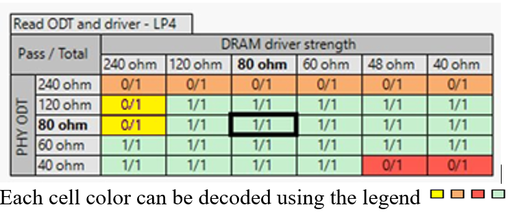
DQ ODT and driver strength tests sweep the DQ IO configurations to create board-specific Driver Strength vs. ODT PASS/FAIL map for the Reads and the Writes.
Note: Optimization is not available when UI configuration is bypassed by RPA initialization script import.
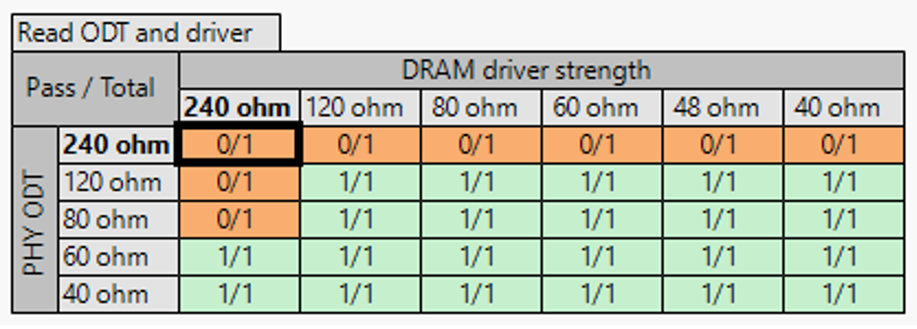
DQ ODT and DS map#
For passing cells (Green cells), the option Apply current selection in DDR configuration (right-click on the cell) is enabled. It sets the respective Driver Strength and ODT value into the configuration for use in other scenarios.

Apply DQ ODT and DS configuration#
Note: You can use the Driver Strength vs. ODT map as one of the criteria when deriving optimal ODT/Driver Strength values. This map cannot serve as all-comprising output to make this determination.
Note: NXP strongly recommends using the default ODT and Drive strength values that are tested and validated as part of our GA BSP. To ensure that your design adheres to the board layout requirements, refer to the device i.MX 8M Hardware Developer’s Guide.
Vref for 1D optimization test sweeps the PHY Vref and/or DRAM Vref to determine the values for the PHY training to pass in case PHY training fails and to determine the trained values after the 2D training.
When the test passes, Apply current selection in DDR configuration option is enabled. It sets the respective PHY Vref and DRAM Vref values into the configuration.
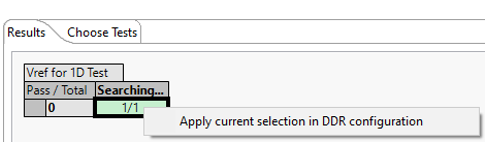
Apply current selection in DDR configuration#
Vref for the CA optimization test executes only 1D training and reads the VrefCA after the training is complete.
When the test passes, the Apply the current selection in the DDR configuration option, which sets the VrefCA value into the configuration, is enabled.
vTSA#
vTSA performs Virtual Timing Signal Analysis by running tests to determine margins of DDR subsystem.
Diag Write Margin/ Diag Read Margin tests creates virtual data eye diagram for each DQ lanes.
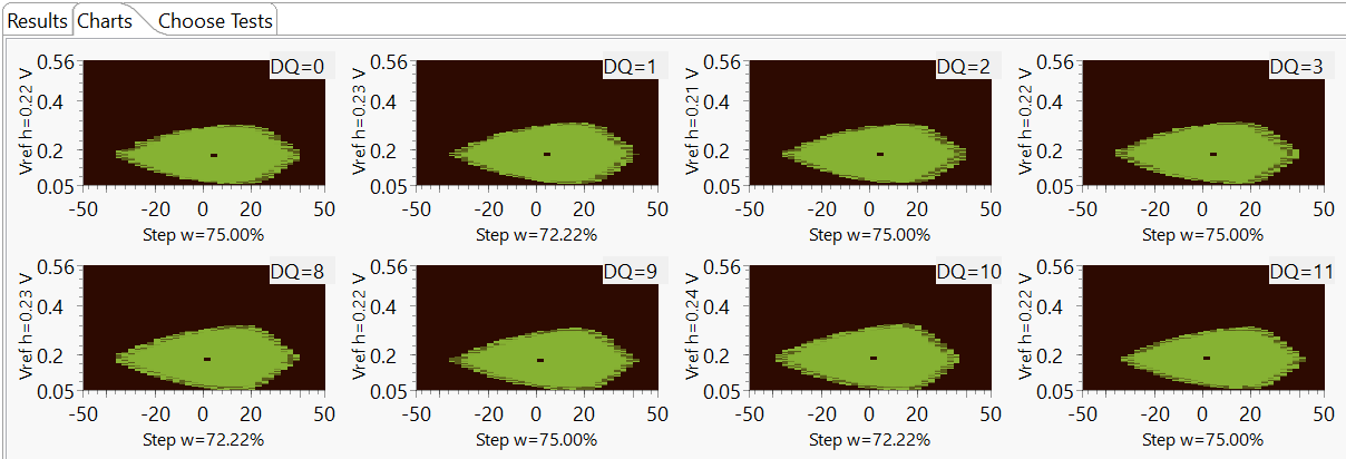
Diagnostic data eyes#
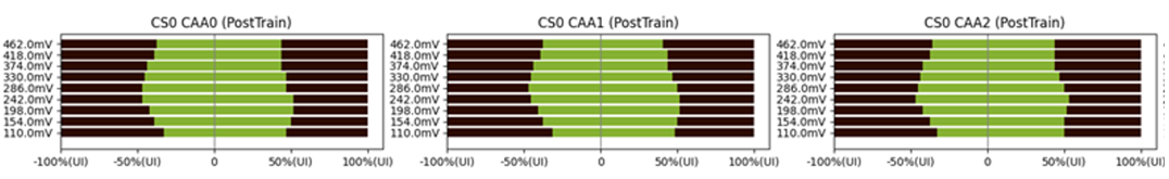
CA bus signals test creates post training diagrams of the 6 CA control lines for each channel and CS.
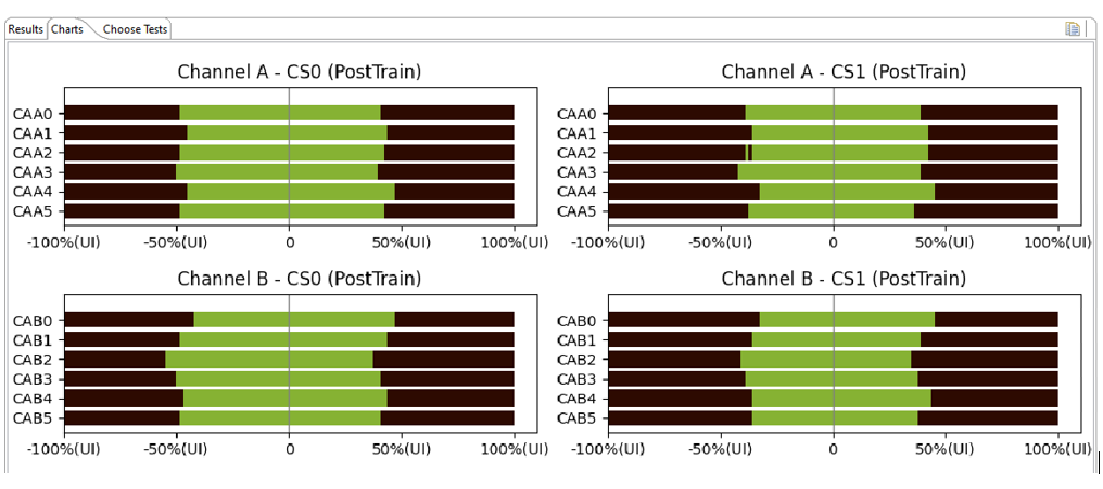
Diagrams of the 6 CA control lines#
CA eye test creates post training eyes of the 6 CA control lines for each channel and CS.
Command/Address eye#
Note: Details about vTSA are provided in the FAQ section.
Stressing#
To test the stability of the DDR configuration more extensively, you can use the Stressing scenario, with its suite of tests that covers different situations.
Two ways of running Stress tests are available:
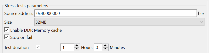
Single run runs the test suite one time with different options selected (Size, Enable DDR Memory cache, Stop on fail). In case of failure, you can check the status of each test in the suite in the Logs console, with Log level set to INFO
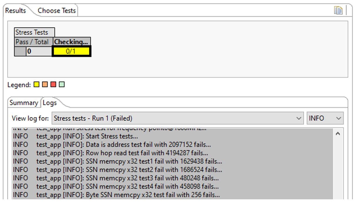
Stress tests#
Test duration runs the test suite for a selected time. This is suitable for overnight tests.
Stress tests options#
In the Logs console, you can monitor test execution and see the number of iterations and the duration.
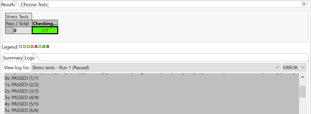
Stress tests results#
Note: Make sure the Timeout (seconds) setting is higher than the Test duration setting, otherwise the test ends with timeout.
FAQ#
What does vTSA mean?
vTSA is an abbreviation for Virtual Timing Signal Analysis.
A “virtual” TSA uses the memory controller itself to test margins without test equipment. “Virtual” does not mean simulation!
Memory controllers have the ability the alter timings, voltage references, termination settings, and so on, for both incoming and outgoing signals.
“Training” is a process when the memory controller sweeps these parameters and finds the configuration with the most margin for operation.
A vTSA simply logs this information for output, which provides insight into the signaling margin of the system without the need for test equipment.
Initialization and calibration settings can be dumped to a file for analysis as well.
What is the vTSA output?
Virtual Timing Signal Analysis(vTSA) provides write and read data eye diagrams virtually by running a series of write/read transactions as opposed to the hardware method of using a high-speed oscilloscope to perform manual physical TSA (pTSA) measurements.
This being the case, vTSA output itself approximates the actual write/read eyes.
You should expect some variation between trained values of delay lines and VREF in comparison to the vTSA report of these values.
vTSA only reports the values it detects in the “widest” part of the reported eye, which may itself vary from run-to-run.
The key takeaway from using this tool is to display the virtual write/read eyes to convince the user of the robustness of their design.
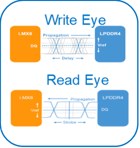
Read eye#
Need more information about vTSA?
The vTSA tool is an approximation of an actual pTSA. Thus, you may note some variation between the trained delay line value and the vTSA “mid” value. It is observed and expected that this variation may be up to ~20 ps. The key takeaway from the generated eye diagrams should be focused on verifying the ample margin of the trained delay line value within the data eye.
For the trained VREF value, the LPDDR4 device Mode Register 14 (MR14 which holds the trained VREF value) applies to ALL byte lanes. In other words per JEDEC, there is not an MR14 per byte lane and instead, MR14 applies to all byte lanes.
For a board that follows the NXP DDR layout guidelines, there should be plenty of margin around the VREF trained value. You can find the guidelines in the respective NXP Hardware Developer Guide.
How a data eye margin is generated?
There are several delay steps available to shift each DQ and DQS.
As DQ crosses the unit interval, from zero-step delay to 1 unit internal step delay, each step is tested with a write-read-compare test to determine pass or fail.
The DQ traverse of the unit interval is repeated for all available VREF steps.
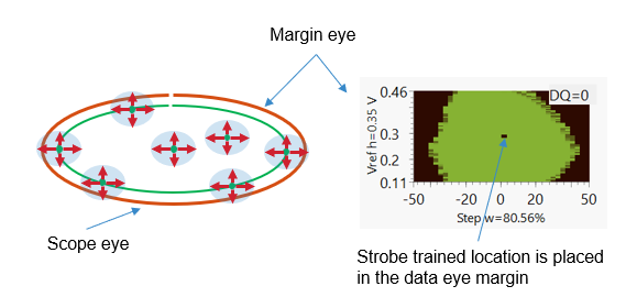
Delay steps generate a line, and repeating the lines at each VREF step generates data eye margin.
The crossing of DQS signal with trained VREF and delay step is placed in the generated data eye margin.
Each passing dot in the margin eye already meets the setup, hold, and voltage requirement.
Data eye margin generation#
What represents the information next to the data eye?
Unit interval = 1/data rate; for example, at 3200MT/s data rate the unit interval = 312.5 ps
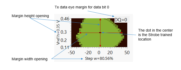
The x-axis displays the time. It is one unit interval in percentage. -50 % to +50 %
The x-axis data eye margin width opening is displayed as the percentage of one unit interval. For example: Step w=80.56 % of UI
The y-axis displays the voltage.
The y-axis open data eye margin height/amplitude opening is displayed in voltage. Ex: Vref h=0.35 V
Data eye information#
How much margin is considered as good?
To determine the required margin mask, you must do the following:
Optimize The DDR interface
Settings have been optimized, generate the worst-case data eye margin using the worst-case conditions (temperature, voltage, frequency, pattern) for a customer board DDR interface.
Use the DDR training optimizing/centering the strobe to the eye margin
A green pixel in the data eye margin indicates a passing cell. It means for that green pixel the setup and hold time as well as the VIHLac/dc are satisfactory.
Any additional green pixels around the strobe location in the data eye margin are additional margin available to DDR for that DQ.
Why is the trained Vref sometimes not in the exact center of the eye?
The VREF training must select a value that corresponds to all of the byte lanes’ passing VREF window and then program this value into the LPDDR4 MR14 register. It means that for a one-byte lane, though the trained VREF value may not seem to be in the exact center of the data eye, it is selected to provide the best possible margin for this byte lane along with satisfying the other byte lanes.
How to check that wrong UART is selected?
Set the Log Level to DEBUG and check the messages from console

Wrong UART selected - message 1#
or

Wrong UART selected - message 2#
How to proceed in case of test timeout?